Browse Products
- Low Noise Amplifier
- Wide Band Gain Block
- SOT363/343 Gain Block
- Internally Matched IF Amplifier
- Wide Band Drive Amplifier
- Wide Band Medium Power Amplifier
- High Power Amplifier
- Wide Band RF Switch
- Digital Step Attenuator
- Digital Variable Gain Amplifier
- Mixer
- Divider
- CATV/Settop Box
- IoT(FEM)
- Automotive Products
- pHEMT LNA
- HBT Bare Die
- Power pHEMT Bare Die
- Packaged pHEMT
- MESFET
- GaN HEMT
- Product Benefits
New Products
| No | Part No. | Description | Key Features | |
|---|---|---|---|---|
| Low Noise Amplifier | ||||
| 1 |

BLB04 |
2000–5000 MHz High Linearity LNA |
• Operated at 3.3V and 5.0V • 33.0dBm Output IP3 at 0dBm/tone at 3600MHz • 18.0dB Gain at 3600MHz • 18.7dBm P1dB at 3600MHz • 0.59dB NF at 3600MHz • Fast shut down to support TDD systems • Lead-free/Green/RoHS Compliant DFN8 2x2 Package |
|
| 2 |

BLB28 |
2000–7000 MHz High Gain LNA |
• Operated at 5.0V • 33.0dBm Output IP3 at 0dBm/tone at 3600MHz • 21.5dB Gain at 3600MHz • 20.3dBm P1dB at 3600MHz • 0.69dB NF at 3600MHz • Fast shut down to support TDD systems • Lead-free/Green/RoHS Compliant DFN8 2x2 Package |
|
| Wide Band Gain Block | ||||
| 1 |

BBA31 |
50-5000 MHz Flat Gain BroadBand AMP |
• Gain = 14.8 dB @ 900MHz • OIP3 = 40.8 dBm @ 900 MHz • Output P1 dB = 22.2 dBm @ 900 MHz • N.F = 1.95dB @ 900 MHz • Internally matched to 50 ohms • Green/RoHS2 Compliant DFN 8L 2x2 Package |
|
| 2 |

BGM26 |
1700-6000 MHz Gain Block 2stage AMP |
• Gain = 31.0 dB @ 3500MHz • OIP3 = 30.0 dBm @ 3500MHz • Output P1 dB = 19.5 dBm @ 3500 MHz • 5GNR ACLR = 8.9 dBm @ 3500MHz • Internally matched to 50 ohms • Fast shut down to support TDD systems • Green/RoHS2 Compliant QFN 16L 3x3 Package |
|
| SOT363/343 Gain Block | ||||
| 1 |

BGH5 |
40-6000 MHz BROADBAND AMPLIFIER |
• Single Fixed 3.3V supply • Gain = 14.0 dB @ 3500MHz • Output P1 dB = 14.0 dBm @ 3500MHz • 5G NR ACLR = 2.5 dBm @ 3500MHz • Internally matched to 50 ohms • RoHS2-compliant SOT-363 SMT package |
|
| Wide Band RF Switch | ||||
| 1 |

BSW7221V |
5-8500MHz Low Loss / Fast Switching SPDT RF switch for Automotive |
• AEC-Q100 Grade 2 Qualified (1st Lot) • Frequency range : 5 MHz to 8.5 GHz • Fast Switching Time : 90 to 135 ns • Supply Voltage : 2.7V to 3.6V • Low insertion loss : 0.37dB @ 2.45GHz / 0.59dB @ 5.75GHz • High isolation : 44dB @ 2.45GHz / 29dB @ 5.75GHz • Input 1 dB output compression : 37dBm @ 2.45GHz / 35dBm @ 5.75GHz / 34dBm @ 8.00GHz • High IIP3 : 65dBm @ 2.45GHz / 62dBm @ 5.75GHz • ESD protection : HBM 2.0kV / CDM 1.0kV • 6-Lead UDFN package : 1.5mm x 1.5mm x 0.5mm • Operating temperature range : -40°C to +105°C • Lead-free/RoHS2-compliant UDFN package |
|
| 2 |

BSW6620 |
5-8000MHz Ultra High Isola on SPDT RF Switch |
• Output frequency range : 5MHz to 8.0GHz • Supply Voltage : 2.7V to 5.5V • ESD, HBM : ±2.0kV @All pins • Opera ng temperature range : -40°C to +105°C • Low Insertion Loss : 0.78dB @ 2GHz / 0.74dB @ 4GHz / 0.92dB @ 6GHz • Ultra High Isolation - RFC to RFx : 65dB @ 2GHz / 58dB @ 4GHz / 54dB @ 6GHz - RFx to RFx : 56dB @ 2GHz / 50dB @ 4GHz / 46dB @ 6GHz • Switching me : 120 to 240ns • 16-Lead QFN package : 4.0mm x 4.0mm x 0.9mm • Lead-free/RoHS2 compliant QFN package |
|
| 3 |

BSW6622 |
5-8000MHz Ultra High Isola on SPDT RF Switch |
• Output frequency range : 5MHz to 8.0GHz • Supply Voltage : 2.7V to 5.5V • ESD, HBM : ±1.5kV @All pins • Opera ng temperature range : -40°C to +105°C • Low Insertion Loss : 0.73dB @ 2GHz / 0.87dB @ 4GHz / 1.10dB @ 6GHz • Ultra High Isolation - RFC to RFx : 62dB @ 2GHz / 57dB @ 4GHz / 48dB @ 6GHz - RFx to RFx : 72dB @ 2GHz / 58dB @ 4GHz / 48dB @ 6GHz • Switching me : 120 to 220ns • 20-Lead QFN package : 4.0mm x 4.0mm x 0.9mm • Lead-free/RoHS2 compliant QFN package |
|
| Digital Variable Gain Amplifier | ||||
| 6Bit Attenuation Control : 0.5dB step | ||||
| 1 |

BVA518C |
5-4000MHz Wide Band Digital Variable Gain Amplifier |
• Integrate DSA to Amp Functionality • Power Supply Range AMP : Nominal 5.0V DSA : 2.7V to 5.5V • 5-4000MHz Broadband Performance • 20.0dB Gain @ 1.9GHz • 5.3dB Noise Figure at max gain setting @ 1.9GHz • 19dBm P1dB @ 1.9GHz • 32.7dBm OIP3 @ 1.9GHz • No matching circuit needed • Attenuation: 0.5 dB steps up to 31.5 dB • Safe attenuation state transitions • High attenuation accuracy (DSA to Amp) ±(0.25 + 3% x ATT) @ 1.9GHz • 1.8V control logic compatible • Programming modes - Direct Parallel - Latched Parallel - Serial • Unique power-up state selection • Lead-free/RoHS2-compliant 24-lead 4mm x 4mm x 0.9mm QFN SMT package |
|
| 7Bit Attenuation Control : 0.25dB step | ||||
| 2 |
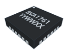
BVA1761 |
50-6000MHz High Linearity wideband DVGA with addressable function |
• Integrate DSA to AMP Functionality • 50-6000MHz Broadband Performance • Wide VDD Range AMP : 3.3V to 5.25V DSA : 2.7V to 5.5V • Low current : 85mA @ 5V, 48mA @ 3.3V • High Gain 18.7dB @ 1.9GHz, 17dB @ 3.5GHz (VDD=5V) 18.2dB @ 1.9GHz, 16.5dB @ 3.5GHz (VDD=3.3V) • High OP1dB 20.8dBm @ 1.9GHz, 20.0dBm @ 3.5GHz (VDD=5V) 17.9dBm @ 1.9GHz, 16.8dBm @ 3.5GHz (VDD=3.3V) • High OIP3 36.9dBm @ 1.9GHz, 37.5dBm @ 3.5GHz (VDD=5V) 33.3dBm @ 1.9GHz, 33.4dBm @ 3.5GHz (VDD=3.3V) • Noise Figure at max gain setting 2.1dB @ 1.9GHz, 2.8dB @ 3.5GHz • Attenuation Range : Up to 31.75dB / 0.25dB step • Safe attenuation state transitions • Excellent attenuation accuracy ±(0.25 + 3% x ATT) @ 1.9GHz ±(0.25 + 5% x ATT) @ 3.5GHz • Programming modes Serial mode only to minimize Control line • 3bit Addressable function LE/DATA/CLK can be shared up to 8EA Chips • Lead-free/RoHS2-compliant 24-lead 4mm x 4mm x 0.9mm QFN SMT package |
|
| 3 |
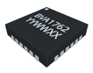
BVA1762 |
500-8000MHz Ultra Flat Gain wideband DVGA with addressable function |
• Integrate DSA to AMP Functionality • 500-8000MHz Broadband Performance • Wide VDD Range AMP : 4.0V to 5.25V DSA : 2.7V to 5.5V • Low current : 110mA @ 5V, 55mA @ 4V • High Gain 20.4dB @ 1.9GHz, 19.7dB @ 3.5GHz (VDD=5V) 19.5dB @ 1.9GHz, 19.1dB @ 3.5GHz (VDD=4V) • High OP1dB 20.8dBm @ 1.9GHz, 20.7dBm @ 3.5GHz (VDD=5V) 19.2dBm @ 1.9GHz, 19.1dBm @ 3.5GHz (VDD=4V) • High OIP3 36.0dBm @ 1.9GHz, 34.9dBm @ 3.5GHz (VDD=5V) 32.5dBm @ 1.9GHz, 32.9dBm @ 3.5GHz (VDD=4V) • Noise Figure at max gain setting 2.6dB @ 1.9GHz, 3.2dB @ 3.5GHz • Attenuation Range : Up to 31.75dB / 0.25dB Step • Safe attenuation state transitions • Excellent attenuation accuracy ±(0.25 + 3% x ATT) @ 1.9 GHz ±(0.25 + 5% x ATT) @ 3.5 GHz • Programming modes Serial mode only to minimize Control line • 3bit Addressable function LE/DATA/CLK can be shared up to 8EA Chips • Lead-free/RoHS2-compliant 24-lead 4mm x 4mm x 0.9mm QFN SMT package |
|
| 4 |

BVA2761 |
50-6000MHz High Gain, High Linearity wideband DVGA with addressable function |
• Integrate AMP1 + DSA + AMP2 Functionality • 50-6000MHz Broadband Performance • Wide VDD Range AMP1 & AMP2 : 3.3V to 5.25V DSA : 2.7V to 5.5V • Low current : 166mA @ 5V, 96mA @ 3.3V • High Gain 38.2dB @ 1.9GHz, 34.8dB @ 3.5GHz (VDD=5V) 37.3dB @ 1.9GHz, 33.4dB @ 3.5GHz (VDD=3.3V) • High OP1dB 21.6dBm @ 1.9GHz, 20.7dBm @ 3.5GHz (VDD=5V) 18.6dBm @ 1.9GHz, 17.4dBm @ 3.5GHz (VDD=3.3V) • High OIP3 36.8dBm @ 1.9GHz, 36.6dBm @ 3.5GHz (VDD=5V) 34.1dBm @ 1.9GHz, 34.4dBm @ 3.5GHz (VDD=3.3V) • Excellent Noise Figure 1.3dB @ 1.9GHz, 1.5dB @ 3.5GHz (ATT=0dB) 2.9dB @ 1.9GHz, 4.2dB @ 3.5GHz (ATT=15.75dB) • Attenuation Range : Up to 31.75dB / 0.25dB step • Safe attenuation state transitions • Excellent attenuation accuracy ±(0.25 + 3% x ATT) @ 1.9 GHz ±(0.25 + 5% x ATT) @ 3.5 GHz • Programming modes Serial mode only to minimize Control line • 3bit Addressable function LE/SI(DATA)/CLK can be shared up to 8EA Chips • Lead-free/RoHS2-compliant 32-lead 5mm x 5mm x 0.9mm QFN SMT package |
|
| 5 |
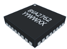
BVA2762 |
500-8000MHz Ultra Flat, High Gain Wideband DVGA with addressable function |
• Integrate AMP1 + DSA + AMP2 Functionality • 500 - 8000MHz Broadband Performance • Wide VDD Range AMP1 & AMP2 : 4.0V to 5.25V DSA : 2.7V to 5.5V • Low Current : 215mA @ 5V, 110mA @ 4V • High Gain 41.5dB @ 1.9GHz, 40.5dB @ 3.5GHz (VDD=5V) 39.9dB @ 1.9GHz, 39.0dB @ 3.5GHz (VDD=4V) • High OP1dB 21.3dBm @ 1.9GHz, 21.2dBm @ 3.5GHz (VDD=5V) 19.1dBm @ 1.9GHz, 19.5dBm @ 3.5GHz (VDD=4V) • High OIP3 36.3dBm @ 1.9GHz, 35.6dBm @ 3.5GHz (VDD=5V) 31.3dBm @ 1.9GHz, 32.8dBm @ 3.5GHz (VDD=4V) • Excellent Noise Figure 1.5dB @ 1.9GHz, 1.8dB @ 3.5GHz (ATT=0dB) 3.2dB @ 1.9GHz, 3.4dB @ 3.5GHz (ATT=15.75dB) • Attenuation Range : Up to 31.75dB / 0.25dB step • Safe attenuation state transitions • Excellent attenuation accuracy ±(0.25 + 3% x ATT) @ 1.9GHz ±(0.25 + 5% x ATT) @ 3.5GHz • Programming modes Serial mode only to minimize Control line • 2bit Addressable function LE/DATA/CLK can be shared up to 4EA Chips • Lead-free/RoHS2-compliant 32-lead 5mm x 5mm x 0.9mm QFN SMT package |
|
| 6 |
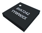
BVA7242 |
3000-4200MHz High linearity Flat Gain Digital Variable Gain Amplifier |
• Integrated AMP1 + DSA + AMP2 • Frequency Range : 3.0GHz - 4.2GHz • Wide VDD Range : 3.3V to 5.25V • Low Current : 98mA @ 3.3V, 170mA @ 5.0V • High Gain : 34.5dB Gain @ 3.6GHz • Excellent Gain Flatness Under 0.8dB @ 800MBW (3.2 - 4GHz) • 1.8dB Noise Figure @ 3.6GHz, ATT = 0dB (Max gain ) • 20dBm Output P1dB @ 3.6GHz , VDD = 5.0V • High Output IP3 @ VDD = 5.0V 38dBm @3.6GHz, ATT = 0dB (Max gain) 35.5dBm @3.6GHz, ATT = 15dB • Attenuation Range : 0 - 31.75 dB / 0.25 dB step • Glitch-less attenuation state during transitions • High attenuation accuracy ±(0.25dB + 5% x ATT. Setting) @ 3.2 - 4.0GHz • Serial Programming Interface only • Power Down Mode (P/D) • Lead-free/RoHS2-compliant 28-pin 6mm x 6mm x 1.07mm LGA SMT Package |
|
| Divider | ||||
| 1 |

|
2700-6000MHz WLAN & 5G WideBand 2-Way SMT Power Divider |
• Typical Isolation = 25.5 dB @ 4.9GHz • Typical Insertion Loss = 0.8 dB @ 4.9GHz • Typical Amplitude Diff. = 0.02 @ 4.9GHz • Typical Phase Diff. = 1.6 @ 4.9GHz • RoHS2-compliant 12L QFN 3x3 Plastic Package |
|
| IoT(FEM) | ||||
| 1 |
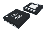
8TR1212 |
2.4-2.485GHz 2.4GHz ZigBee / Thread / Bluetooth Smart Front End RFIC |
• 2.4-2.485GHz Frequency Range • High Efficiency Optimized for Battery Operation • Delivers up to +10.6dBm Output Power at 3.3V • 10.3mA at +10dBm Output Power at 3.3V • Large Signal Gain 13.8dB at +10dBm Output Power • 1.8 - 4.0V Operation • Integrated PA, Bypass, T/R Switch • -40℃ to 125℃ Extended Temperature Range • 2mm x 2mm x 0.45mm 8-Pin DFN Package |
|
| 2 |
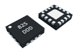
8TR8217 |
2.4-2.485GHz 2.4GHz ZigBee / Thread / Bluetooth Smart Front End RFIC |
• 2.4 - 2.485GHz Frequency Range • High Efficiency Optimized for Battery Operation • Delivers up to +23dBm Output Power at 3.3V • 160mA at +23dBm Output Power at 3.3V • 1.6dB LNA Noise Figure at RX mode • 2.7 - 4.0V Opera on • Single-Ended Transceiver Interface • -40°C to 125°C Extended Temperature Range • 3mm x 3mm x 0.45mm 16-Pin QFN Package |
|
| 3 |

8TR8218 |
2.4-2.485GHz 2.4GHz ZigBee / Thread / Bluetooth Smart Front End RFIC |
• 2.4 - 2.485GHz Frequency Range • High Efficiency Optimized for Battery Operation • Delivers up to +23dBm Output Power at 3.3V • 160mA at +23dBm Output Power at 3.3V • 1.6dB LNA Noise Figure at High current mode • 2.7 - 4.0V Opera on • Single-Ended Transceiver Interface • -40°C to 125°C Extended Temperature Range • 3mm x 3mm x 0.45mm 16-Pin QFN Package |
|
| 4 |
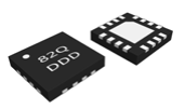
8TR8219 |
2.4-2.485GHz 2.4GHz ZigBee / Thread / Bluetooth Smart Front End RFIC |
• 2.4 - 2.485GHz Frequency Range • High Efficiency Optimized for Battery Operation • Delivers up to +23dBm Output Power at 3.3V • 160mA at +23dBm Output Power at 3.3V • 1.9dB RX LNA Noise Figure • 2.7 - 4.0V Opera on • Single-Ended Transceiver Interface • -40°C to 125°C Extended Temperature Range • 3mm x 3mm x 0.45mm 16-Pin QFN Package |
|


